- 您现在的位置:买卖IC网 > Sheet目录3882 > PIC16F87T-E/ML (Microchip Technology)IC MCU FLASH 4KX14 EEPROM 28QFN
74
8008H–AVR–04/11
ATtiny48/88
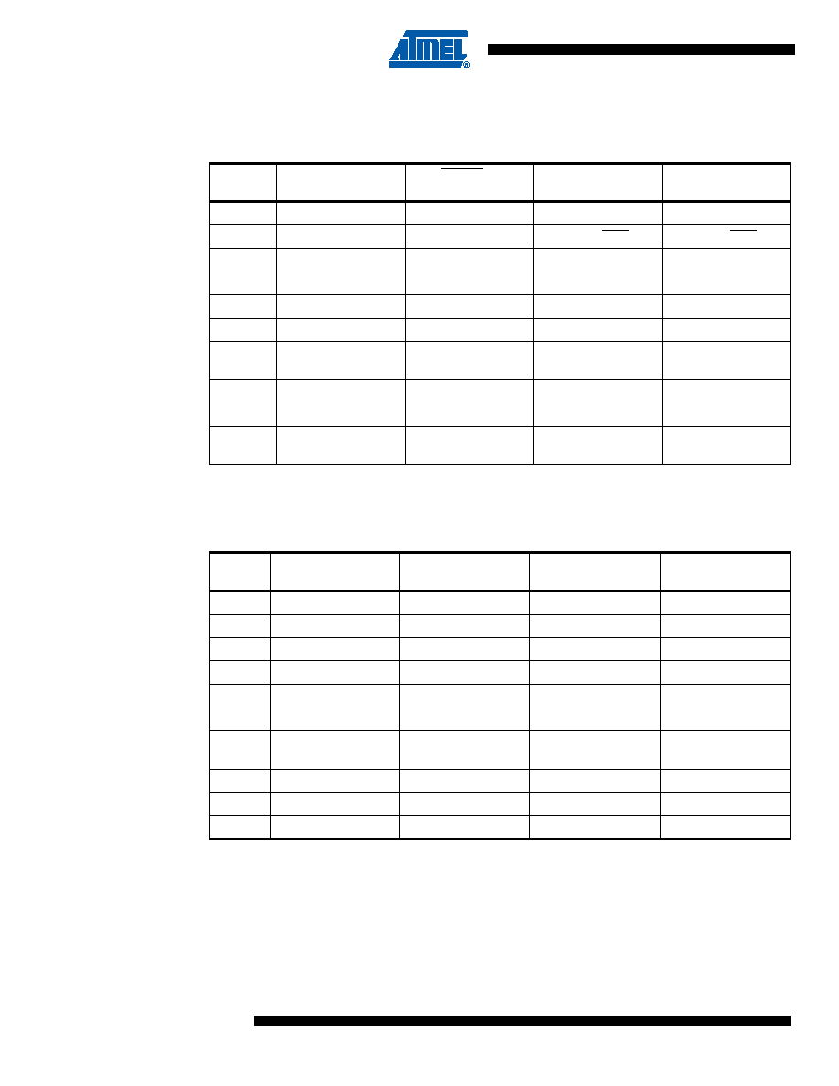
Table 10-9 and Table 10-10 relate the alternate functions of Port C to the overriding signals
shown in Figure 10-6 on page 66.
Note:
1. When enabled, the 2-wire Serial Interface enables slew-rate controls on the output pins PC4
and PC5. This is not shown in the figure. In addition, spike filters are connected between the
AIO outputs shown in the port figure and the digital logic of the TWI module.
Table 10-9.
Overriding Signals for Alternate Functions in PC[6:4](1)
Signal
Name
PC7/PCINT15
PC6/RESET/
PCINT14
PC5/SCL/ADC5/
PCINT13
PC4/SDA/ADC4/
PCINT12
PUOE
0
RSTDISBL
TWEN
PUOV
0
1
PORTC5 PUD
PORTC4 PUD
DDOE
0
RSTDISBL
TWEN
DDOV
0
SCL_OUT
SDA_OUT
PVOE
0
TWEN
PVOV
0000
DIEOE
PCINT15 PCIE1
RSTDISBL +
PCINT14 PCIE1
PCINT13 PCIE1 +
ADC5D
PCINT12 PCIE1 +
ADC4D
DIEOV
1
RSTDISBL
PCINT13 PCIE1
PCINT12 PCIE1
DI
PCINT15 INPUT
PCINT14 INPUT
PCINT13 INPUT
PCINT12 INPUT
AIO
-
RESET INPUT
ADC5 INPUT / SCL
INPUT
ADC4 INPUT / SDA
INPUT
Table 10-10. Overriding Signals for Alternate Functions in PC[3:0]
Signal
Name
PC3/ADC3/
PCINT11
PC2/ADC2/
PCINT10
PC1/ADC1/
PCINT9
PC0/ADC0/
PCINT8
PUOE
000
0
PUOV
000
0
DDOE
0
DDOV
0
PVOE
000
0
PVOV
000
0
DIEOE
PCINT11 PCIE1 +
ADC3D
PCINT10 PCIE1 +
ADC2D
PCINT9 PCIE1 +
ADC1D
PCINT8 PCIE1 +
ADC0D
DIEOV
PCINT11 PCIE1
PCINT10 PCIE1
PCINT9 PCIE1
PCINT8 PCIE1
DI
PCINT11 INPUT
PCINT10 INPUT
PCINT9 INPUT
PCINT8 INPUT
AIO
ADC3 INPUT
ADC2 INPUT
ADC1 INPUT
ADC0 INPUT
发布紧急采购,3分钟左右您将得到回复。
相关PDF资料
PIC16F87-E/ML
IC MCU FLASH 4KX14 EEPROM 28QFN
PIC18LF4320-I/ML
IC MCU FLASH 4KX16 EEPROM 44QFN
PIC16F77T-I/PTG
IC MCU FLASH 8KX14 W/AD 44TQFP
PIC16LF1933-I/SO
IC PIC MCU FLASH 4K 28-SOIC
PIC16C54C-20I/SO
IC MCU OTP 512X12 18SOIC
PIC16LF726-I/SO
IC PIC MCU FLASH 8K 1.8V 28-SOIC
PIC12CE673-10/P
IC MCU OTP 1KX14 A/D&EE 8DIP
PIC16F726-I/SO
IC PIC MCU FLASH 8KX14 28-SOIC
相关代理商/技术参数
PIC16F87T-E/SO
功能描述:8位微控制器 -MCU 20MHz 4K Flash RoHS:否 制造商:Silicon Labs 核心:8051 处理器系列:C8051F39x 数据总线宽度:8 bit 最大时钟频率:50 MHz 程序存储器大小:16 KB 数据 RAM 大小:1 KB 片上 ADC:Yes 工作电源电压:1.8 V to 3.6 V 工作温度范围:- 40 C to + 105 C 封装 / 箱体:QFN-20 安装风格:SMD/SMT
PIC16F87T-E/SS
功能描述:8位微控制器 -MCU 20MHz 4K Flash RoHS:否 制造商:Silicon Labs 核心:8051 处理器系列:C8051F39x 数据总线宽度:8 bit 最大时钟频率:50 MHz 程序存储器大小:16 KB 数据 RAM 大小:1 KB 片上 ADC:Yes 工作电源电压:1.8 V to 3.6 V 工作温度范围:- 40 C to + 105 C 封装 / 箱体:QFN-20 安装风格:SMD/SMT
PIC16F87T-I/ML
功能描述:8位微控制器 -MCU 7KB 368 RAM 16 I/O RoHS:否 制造商:Silicon Labs 核心:8051 处理器系列:C8051F39x 数据总线宽度:8 bit 最大时钟频率:50 MHz 程序存储器大小:16 KB 数据 RAM 大小:1 KB 片上 ADC:Yes 工作电源电压:1.8 V to 3.6 V 工作温度范围:- 40 C to + 105 C 封装 / 箱体:QFN-20 安装风格:SMD/SMT
PIC16F87T-I/SO
功能描述:8位微控制器 -MCU 7KB 368 RAM 16 I/O RoHS:否 制造商:Silicon Labs 核心:8051 处理器系列:C8051F39x 数据总线宽度:8 bit 最大时钟频率:50 MHz 程序存储器大小:16 KB 数据 RAM 大小:1 KB 片上 ADC:Yes 工作电源电压:1.8 V to 3.6 V 工作温度范围:- 40 C to + 105 C 封装 / 箱体:QFN-20 安装风格:SMD/SMT
PIC16F87T-I/SS
功能描述:8位微控制器 -MCU 7KB 368 RAM 16 I/O RoHS:否 制造商:Silicon Labs 核心:8051 处理器系列:C8051F39x 数据总线宽度:8 bit 最大时钟频率:50 MHz 程序存储器大小:16 KB 数据 RAM 大小:1 KB 片上 ADC:Yes 工作电源电压:1.8 V to 3.6 V 工作温度范围:- 40 C to + 105 C 封装 / 箱体:QFN-20 安装风格:SMD/SMT
PIC16F882-E/ML
功能描述:8位微控制器 -MCU 3.5KB Enh FLSH 128 RAM RoHS:否 制造商:Silicon Labs 核心:8051 处理器系列:C8051F39x 数据总线宽度:8 bit 最大时钟频率:50 MHz 程序存储器大小:16 KB 数据 RAM 大小:1 KB 片上 ADC:Yes 工作电源电压:1.8 V to 3.6 V 工作温度范围:- 40 C to + 105 C 封装 / 箱体:QFN-20 安装风格:SMD/SMT
PIC16F882-E/SO
功能描述:8位微控制器 -MCU 3.5KB Enh FLSH 128 RAM RoHS:否 制造商:Silicon Labs 核心:8051 处理器系列:C8051F39x 数据总线宽度:8 bit 最大时钟频率:50 MHz 程序存储器大小:16 KB 数据 RAM 大小:1 KB 片上 ADC:Yes 工作电源电压:1.8 V to 3.6 V 工作温度范围:- 40 C to + 105 C 封装 / 箱体:QFN-20 安装风格:SMD/SMT
PIC16F882-E/SP
功能描述:8位微控制器 -MCU 3.5KB Enh FLSH 128 RAM RoHS:否 制造商:Silicon Labs 核心:8051 处理器系列:C8051F39x 数据总线宽度:8 bit 最大时钟频率:50 MHz 程序存储器大小:16 KB 数据 RAM 大小:1 KB 片上 ADC:Yes 工作电源电压:1.8 V to 3.6 V 工作温度范围:- 40 C to + 105 C 封装 / 箱体:QFN-20 安装风格:SMD/SMT